

The photovoltaic cell
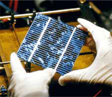
The conversion of solar radiation into an electron current takes place in the photovoltaic cell, a device consisting of a thin sheet of semiconductor metal, very often made of suitably treated silicon.
This treatment is characterised by various chemical processes including so-called "doping".
Adding impurities, that is atoms of boron and phosphorous, to the crystalline structure of the silicon generates an electrical field and produces the charges necessary for the formation of an electrical current. This is created when the cell, whose two faces are connected to a user, is exposed to the light.
The energy which can then be exploited depends on the characteristics of the material the cell is made of: conversion efficiency (the percentage of energy contained in the sunlight incident on the cell which is transformed into electrical energy by the photovoltaic device) for commercial silicon cells generally lies between 13% and 17%, while laboratory cells have produced a reading of 32.5%.
In practice, the typical photovoltaic cell has an overall thickness of between 0.25 and 0.35 mm and is made of mono or multi-crystalline silicon. Generally square, it has a surface measuring somewhere between 100 and 225 m² and, with an irradiation of 1 KW/m² at a temperature of 25°C, produces a current of between 3 and 4 A and a voltage of approximately 0.5V, generating 1.5-2 Wp of power.
The watt peak
As the power of a photovoltaic cell varies with changes in its temperature and radiation, standard parameters have been defined, producing the so-called watt peak (Wp) relating to the power supplied by the cell at a temperature of 25°C and a radiation of 1000 W/m², in AM1 conditions.
As well as crystalline type silicon, there has recently been a great deal of interest shown by various manufacturers in producing modules based on amorphous silicon. Actually, it is not strictly correct to refer to cells when talking about amorphous silicon, as it is generally deposited in layers on sometimes quite large surfaces.
As far as cost is concerned, traditional amorphous silicon costs less than (mono or multi) crystalline silicon, while the cost of amorphous silicon with two or three junctions should come down if it is to be used on a large scale.
The "PHYSICS" of the photovoltaic process
The direct conversion of solar energy into electrical energy, achieved with photovoltaic cells, exploits the physical phenomenon of the interaction of light radiation with valence electrons in semiconductor materials. This is known as the photovoltaic effect. Whatever the material used, the mechanism by which the cell transforms sunlight into electrical energy is essentially unvarying. Let's consider, for the sake of simplicity, the case of a conventional photovoltaic cell made of crystalline silicon.
Normally, the silicon atom has 14 electrons, four of which are in the valence band, and can therefore interact with other atoms, whether they are made of silicon or other elements. Two adjacent atoms belonging to a pure silicon crystal have a couple of electrons in common, one belonging to the considered atom, the other belonging to the adyacent one.
Therefore, there is a strong electrostatic bond between an electron and the two atoms which it helps to keep together. However, this bond may be severed by a sufficient amount of energy.
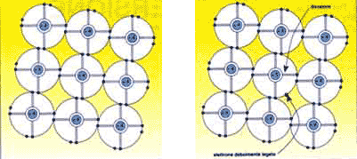
If enough energy is supplied the electron is taken to a higher energy level (conduction band) where it is free to move around, thus contributing to the flow of electricity. When it moves into the conduction band the electron leaves a "hole" behind it, that is a lacuna where an electron is missing. A nearby electron may easily go and fill the hole, thus swapping places with it. To exploit the electricity it is necessary to create a constant movement of electrons (and of holes) , or rather a current, by means of an electrical field inside the cell. The field is produced by special physical and chemical treatments, creating a surplus of positively charged atoms in one part of the semiconductor and a surplus of negatively charged atoms in the other. In practice this condition is obtained by adding small quantities of boron atoms (positively charged) and phosphorous atoms (negatively charged) to the silicon lattice, or in other words doping the semiconductor. The electrostatic attraction between the two kinds of atom creates a fixed electrical field which gives the cell a structure known as "the diode structure", in which the transit of the current, consisting of mobile charge carriers, electrons for instance, is obstructed in one direction and facilitated in the opposite direction. The explanation of this phenomenon can be illustrated as follows.
In the layer doped with phosphorous, which has five valence electrons as opposed to the four in silicon, there is, for each atom of phosphorous, an extra unbonded electron, composed of an so-called valence electron that is free to move around.
In the layer doped with phosphorous, which has five valence electrons as opposed to the four in silicon, there is, for each atom of phosphorous, a weakly bonded negative charge, composed of a so-called valence electron.
Likewise, in the layer doped with boron, which has three outer electrons, there is a surplus positive charge, composed of the holes found in the boron atoms when they bond with silicon.
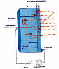
The first, negatively charged layer is labelled N, the second, positively charged layer is labelled P and the border separating them is called junction P-N.
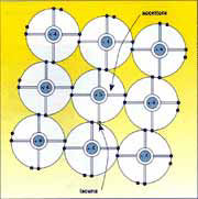
Putting the two layers opposite each other activates an electronic flow from zone N to zone P which, once it has reached the electrostatic point of equilibrium, determines a surplus of positive charge in zone N, due to phosphorous atoms lacking an electron, and an excess of negative charge in zone P, due to electrons migrating from zone N. The result is an electrical field within the device which separates surplus electrons, generated by the absorption of light, from the holes, pushing them in opposite directions (the electrons towards zone N and the holes towards zone P) so that an external circuit can collect the current thus generated.
It is important for the "incorporated" field to be placed as close as possible within the region of the device which absorbs the light. The light photons which have sufficient energy can sever an electron from its bonds and elevate it to a free state in the material's conduction band.
This produces two mobile charge carriers: the free electron, in the conduction band, and the freely moving hole, in the valence band.
The conversion of light into electrical energy by the photovoltaic cell essentially takes place because these light generated mobile charge carriers are pushed in opposite directions by the incorporated electrical field.
Once they have crossed the field, free electrons do not come back, as the field, acting like a diode, prevents them from turning round.
Therefore, when light strikes the photovoltaic cell, positive charges in ever-increasing numbers are pushed towards the top of the cell and negative charges towards the bottom, or vice versa, depending on the type of cell. If the top and bottom are linked by a conductor, mobile charge carriers move across it and we will be able to see an electrical current. For as long as the cell is exposed to the light, electricity flows regularly in the form of continuous current.
Of all the energy which fills the solar cell in the form of light radiation, only a part is converted into electrical energy available to its clamps. Conversion efficiency for commercial silicon cells generally lies between 13% and 17% while laboratory cells have produced a reading of 32.5%.
There are many reasons for this low efficiency, which may be grouped into four categories:
- Reflection: Not all the photons which strike the cell penetrate it, given that some are reflected by the cell's surface and some strike the metal contact grid;
- Photons which are too energetic or not energetic enough: To sever the bond between electron and nucleus a certain amount of energy is required, and not all incident photons have the sufficient energy. On the other hand, photons which have too much energy generate electron-hole pairs, dissipating the surplus energy in the form of heat and splitting the electron from the nucleus.
- Recombination: not every electron-hole pair generated is collected by the electrical field of junction and sent to the external load, given that on the journey between the point of generation and the junction they may meet opposite charges and therefore recombine;
- Parasite resistance: the charges generated and collected in the depletion region must be sent to the outside. They are collected by metallic contacts, placed on the front and back of the cell. When fabricated the silicon and aluminium of the contacts are alloyed but there still remains a certain amount of resistance at the interface which provokes a dissipation that reduces the power transferred to the load. In the case of polycrystalline silicon cells, efficiency is reduced even further due to the resistance the electrons meet on the edge between one grain and another and due to the resistance caused by the random direction of single atoms, even more so in the case of amorphous silicon cells.
The electrical characteristic of solar cells
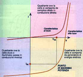
We have already mentioned that the photovoltaic cell is essentially a diode with a large surface. Exposing it to solar radiation the cell behaves like a current generator, whose functioning may be described in terms of its voltage-current characteristic.
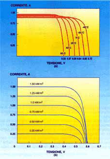
Generally speaking the characteristic of a photovoltaic cell depends on three basic variables; intensity of solar radiation, temperature and area of the cell. The intensity of solar radiation has no significant effect on the open circuit voltage; vice versa the intensity of the short-circuit current varies in proportion to the varying intensity of the irradiation, increasing as this increases.
Temperature has no significant effect on the reading of the short-circuit current. On the contrary, this is proportional to the open circuit voltage, the voltage decreasing as the temperature increases. The cell's area has no effect on the reading of the voltage. Vice versa this is directly proportional to the available current.
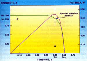
In closed circuit conditions the current generated is maximum (Isc), while in open circuit conditions the voltage is maximum (Voc). In open and closed circuit conditions zero power will be generated as, applying the equation P=V x I, there will be zero current in the first case and zero voltage in the second. At other points power will increase with an increase in voltage, reaching a maximum and decreasing rapidly in proximity to the Voc.
| Mono Si | Multi Si | Amorphous Si | GaAs | CdTe | CIS (CULNSe2) | |
| Cell efficiency | 14-17% | 12-14% | 4-6% single / 7-10% tandem | 32,5% (lab.) | 10% | 12% |
| Benefits | High stable efficiency Reliable technology | < efficiency cost < Easier to fabricate Less space consuming | Cost < need for materials and energy in fabrication, good level of efficiency with low radiation | High resistance to high temperatures (OK for concentrators) | Low cost | Very stable |
| Drawbacks | Cost Grey energy Quantity of material required for fabrication Complexity | Complexity Sensitive to impurities | Low efficiency Initial deterioration Stability over time | Toxicity Availability of material | Toxicity Availability of material | Toxicity (Cd) |
The production of photovoltaic cells
Production methods of photovoltaic cells will differ depending on the type of cell we intend to produce
The major differences lie in the fabrication of the slice of silicon, called the "wafer", which is the principal structure to which various (mainly chemical) treatments are applied, leading to the production of the cell itself.
The monocrystal wafer is produced by the Czochralski method, based on the crystallisation of an extremely pure "seed" of material, which is plunged into the liquid silicon and then extracted and cooled slowly to obtain a monocrystal "ingot", which will be cylindrical in shape (from 13 to 30 cm in diameter and 200 cm in length). This is then doped by adding boron. The ingots are subsequently sliced into wafers measuring between 250 and 350 micrometers thick.
Instead, multicrystal wafers come from the fusion and subsequent re-crystallisation of silicon discarded by the electronics industry (silicon "scraps"). From this fusion we get a "pig", which is then vertically cut into ingots in the shape of parallelepipeds. A subsequent horizontal cut produces slices with a similar thickness to monocrystal cells (250-350 micrometers).
Compared to monocrystal wafers, multicrystal wafers provide a high level of efficiency at a lower cost.
For wafers to become actual photovoltaic cells it is necessary (in the case of both mono and multicrystal wafers):
- to "clean" them by plunging them into soda;
- to add phosphorous atoms (this is N type doping) to the material in order to produce the "p-n junction". This is done by slowly passing the wafers through an oven that "diffuses" orthophosphoric acid, containing the desired phosphorous atoms, into the material;
- to make the front electrical contacts (a metallic grid which collects the electrical charges) and the back surface (a full area metal contact) by screen-printing or electrodeposition, after applying a thin, non-reflective layer (titanium dioxide, TiO2).
- At this point the cell is tested by simulating standard conditions of sunlight (1000 W/m² at 25° with AM1.5 spectrum) in order to classify it and so combine it with cells that have analogous electrical characteristics. This step is very important in order to avoid producing modules with very different cells, which could lead to a drastic reduction in the level of performance of photovoltaic modules.